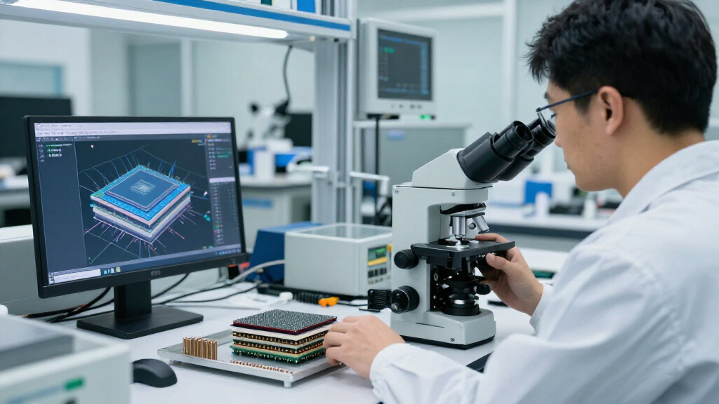
🔍 Read the full analysis: A Three-Dimensional Guide To AI Chip Design And Packaging on ThorstenMeyerAI.com

Get business pricing on monitors, keyboards and dev gear
- Business-only prices and quantity discounts
- Tax-exempt purchasing
- Multiple users, one account, clear invoices
TL;DR
ThorstenMeyerAI.com published a three-dimensional explainer of AI accelerator packaging, tracing components from memory stacks and compute dies to complete server racks. The account highlights how memory bandwidth, advanced packaging capacity and cooling shape the performance and availability of AI systems; some product and supply claims come from manufacturers and remain subject to their stated timelines.
ThorstenMeyerAI.com published a three-dimensional guide to AI accelerator packaging on November 22, showing how compute dies, stacked high-bandwidth memory and silicon interposers fit together—and how those packages scale into liquid-cooled data center racks. The report argues that memory bandwidth and packaging capacity, not just processor speed, can constrain how quickly AI systems are built and run.
The guide uses an open-source CAD model with the layers arranged in their reported order, but schematic dimensions. Its author, Thorsten Meyer, says manufacturers do not publish the physical dimensions of the dies, packages or memory stacks, so the model does not assign guessed measurements. The layers include a package substrate that carries power and signals, a silicon interposer that connects components, compute dies, stacked memory and a liquid-cooling plate.
High-bandwidth memory, or HBM, consists of DRAM dies stacked above a base die and connected vertically by through-silicon vias. The interposer provides dense wiring between the memory and compute dies. TSMC describes its CoWoS-S packaging as using a large silicon interposer to accommodate logic and HBM; for larger designs, CoWoS-L connects silicon bridges within a carrier layer. These packaging methods are part of the manufacturing process, not simply a way to assemble otherwise independent chips.
The report compares vendor descriptions of different accelerators. Nvidia says its Rubin GPU has two reticle-limited compute dies and 336 billion transistors. AMD describes the MI355X as having eight vertically stacked accelerator complex dies and two I/O dies, with eight stacks of 12-high HBM. These are manufacturer specifications cited by the guide; they are not independent measurements. At rack scale, Nvidia’s GB200 and GB300 NVL72 configurations are described as containing 72 GPUs and 36 CPUs, alongside networking, power and cooling hardware.
Packaging Sets the Pace for AI
The guide’s central point is that a fast compute die does not operate in isolation. It must receive data quickly from memory, communicate with other components and shed heat. HBM bandwidth and interposer wiring help keep large workloads supplied with data, while the package’s physical limits determine how many dies and memory stacks can be connected closely together.
That matters beyond chip design. The report cites Nvidia’s product-page figure of 19.2 terabytes per second of memory bandwidth for Rubin, compared with 900 gigabytes per second for the V100. Those are figures for different products and generations, and the guide presents them as a measure of the growth in bandwidth—not as a direct measure of application speed. More broadly, if packaging and memory production cannot keep pace with demand, additional compute designs alone may not translate into more available AI capacity.
Racks also bring power and thermal constraints into the picture. Nvidia identifies 120 kilowatts of cooling capacity for a GB200 NVL72 rack, while its systems route coolant through cold plates attached to processors. The resulting infrastructure requirements affect how data centers are designed and what operators must provide to deploy high-density AI systems.
Products Worth Considering

LG UltraGear 34-Inch Curved QHD Gaming Monitor, 160Hz, FreeSync Premium

Jackery Solar Generator 1000 v2 with 200W Solar Panel, 1024Wh LiFePO4 Battery

Bose QuietComfort Ultra Headphones Gen 1, Lunar Blue
As an affiliate, we earn on qualifying purchases.
From Silicon Layers to Rack Systems
The guide places current packaging in a progression from individual components to full systems. A package substrate forms the base and connects the package to a module or circuit board. Above it, an interposer links compute and memory with much denser connections than a conventional circuit board can provide. HBM towers sit beside the compute dies, while a cold plate handles heat at the top of the assembly.
Manufacturing size limits help explain why interposer designs differ. TSMC says CoWoS-S interposers can reach about 2,700 square millimeters, or 3.3 times a reticle. The guide reports that TSMC said on October 15, 2026, it was in real-world production of five-reticle-size packaging and working on nine- and 14-reticle designs. Those statements describe the company’s reported manufacturing progress, not independently verified output volumes.
At rack level, Nvidia’s GB200 and GB300 NVL72 designs combine 18 compute trays, nine NVLink switch trays, management switches and power shelves. Each compute tray contains two Grace CPUs and four Blackwell GPUs, according to the cited system documentation. The rack view connects package design to deployment: networking, power delivery and liquid cooling all have to work alongside the chips.
“Where AI gets stuck today, it is often not the compute die. It is memory bandwidth, packaging, and how many of these parts the world can actually build.”
— Thorsten Meyer, ThorstenMeyerAI.com
Supply Forecasts and Unpublished Dimensions
The guide does not provide exact physical dimensions for its modeled dies, packages or HBM stacks. Meyer says those measurements are not published by Nvidia or AMD, so the models use schematic sizes. The guide also does not independently verify manufacturers’ specifications, product road maps or production statements.
Actual production capacity and delivery timing remain unclear. SK hynix’s expectation that demand will exceed supply “through 2030” is a forecast attributed to the company. The report gives no detailed supply figures or comparable baseline for that projection. It also does not establish how quickly announced packaging advances or planned products will reach broad commercial availability.
Production Capacity Will Shape Availability
The next developments to watch are manufacturers’ updates on HBM output, advanced packaging capacity and the availability of the accelerator systems described in the guide. TSMC’s stated work on larger CoWoS-L designs and vendor plans for new generations could change how many dies and memory stacks can be integrated, but the guide does not provide a schedule or production volumes for every milestone.
For data center operators, rack deployments will also depend on equipment beyond the accelerators, including power systems, networking and liquid cooling. Future product specifications and supply disclosures will show whether packaging and memory production can keep pace with demand. The article itself is an explainer, not an announcement of a new chip or a change in product availability.
Key Questions
What is the news in this report?
ThorstenMeyerAI.com published a 3D guide showing the layers inside AI accelerators and how packaged chips fit into complete data center racks.
What does HBM do in an AI accelerator?
High-bandwidth memory stores data close to the compute dies. Its DRAM layers are stacked and connected vertically, helping deliver data to the processor over many connections.
Why does packaging matter for AI hardware?
Packaging connects compute, memory and other components. Interposer capacity, memory bandwidth and manufacturing output can limit how systems are built and supplied, even when compute designs advance.
Are the 3D models drawn to exact scale?
No. The author says the model uses schematic dimensions because Nvidia and AMD do not publish the relevant die, package and memory-stack measurements.
What remains uncertain about AI chip supply?
The report does not verify future production volumes or when every announced packaging capability will be widely available. The forecast that memory demand will exceed supply through 2030 is attributed to SK hynix and should be read as the company’s expectation.
Source: ThorstenMeyerAI.com